Feb 18 2013
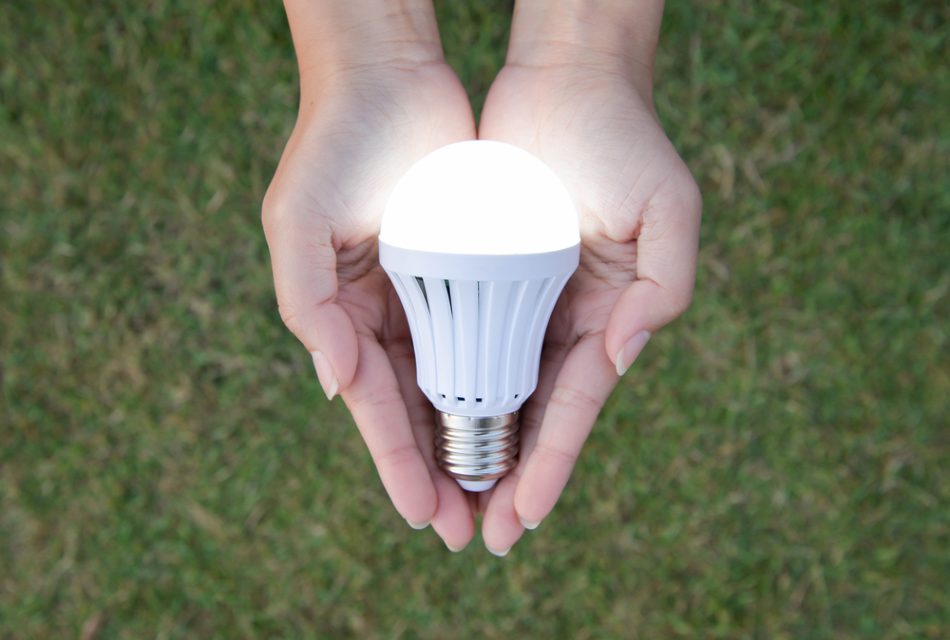
Image Credit: Magnetic Mcc/Shutterstock.com
Article updated on 18/02/20 by Kerry Taylor-Smith
LEDs or light emitting-diodes are light sources that operate when electrons move through a semiconductor material. LEDs can be constructed into different types of lighting products such as light bulbs, flashlights, etc, as well as be used in various types of applications.
LEDs are generally classified into two types:
- Low-powered LEDs – LEDs that draw attention to something such as a colored blinking light on a camera or an exit sign.
- High-powered LEDs – These are used for lighting a specific area. For example, a large number of LEDs are used inside a fixture to produce white light.
Basic Components of LEDs
LED lights comprise of a small chip with semi-conducting material layers. LED packages may contain one or several chips, mounted on a heat-conducting material known as a 'heat sink' which is covered by a lens. The resulting device, normally 7 to 9 mm thickness, can be used in various ways.
The LEDs are then placed on a circuit board that can be programmed to include lighting controls such as light sensing, dimming, and pre-set timing. The circuit board is arranged on another heat sink so that heat from the LEDs is controlled. The system is then enclosed within an architectural structure, lighting fixture or light bulb package.
The Manufacturing Process
The manufacturing process of LEDs is as follows:
Wafer Fabrication
Firstly, a semiconductor wafer is fabricated. The color of the LED decides the material composition to be used, whether GaAs, GaP or something in between. The crystalline semiconductor is grown in a high pressure, high-temperature chamber. Arsenic, gallium and/or phosphor are purified, liquefied and pressed together by heat and pressure so that they form a solution. Then they are subjected to 'Czochralski crystal' growth or a 'liquid encapsulation technique', which involves coating them with a liquid boron oxide layer so that they do not escape. After mixing the elements in a uniform solution, which is cooled and crystallized to form a cylindrical, long crystal ingot of GaP, GaAs or GaAsP.
The boule is cut into fine semiconductor wafers at and they are polished. The efficiency of the LED depends on how well the crystal is formed.
The cleaning of the wafers is done via a rigorous ultrasonic and chemical process using a number of solvents. Dust, dirt or organic matter that may have settled on the surface is removed through this process. The cleaner the processing, the better the resulting LED.
Semiconductor Dopants
Additional semiconductor crystal layers are grown on the wafer surface. Dopants or impurities are added to the crystal. Liquid phase epitaxy (LPE) involves the deposition of epitaxial-semiconductor layers with the same crystalline orientation as the underlying substrate on a wafer, whilst being drawn under molten GaAsP reservoirs. A crystal layer growth technique is applied. LPE creates a highly uniform material layer making it a preferred doping technique with the formed layers being several microns thick.
Additional dopants may be added to vary the diode characteristics for efficiency or color. In case of further doping, the wafer is mounted in a high-temperature furnace tube which is then immersed in a gaseous atmosphere with dopants. The most common dopants are zinc ammonium or nitrogen.
Metal Contact Patterning
In the design stage, a metal contact pattern is determined, which has to be defined on the wafer. The wafer is made to spin and is deposited in drops onto the surface and is then cooled.
Contact metal is evaporated onto the pattern and fills in the exposed areas. Evaporation occurs in a vacuum-sealed, high-temperature chamber. Metal is heated to a temperature that causes it to vaporize, condense and adhere to the exposed semiconductor wafer. Acetone washes away the photoresist leaving only metal contacts. The metal deposited must be annealed, so the wafer is heated to several hundred degrees and kept in a furnace for several hours. At this stage, the semiconductor and metal bond together chemically, ensuring that contacts do not flake off. A single 2-in diameter wafer produced this way will have the same pattern repeated several times offering an indication of the finished diode size. The diodes are separated either by snapping the wafer along the crystal plane or by sawing with a diamond saw. Each segment cut from the wafer is known as a die.
Mounting and Sealing
Individual dies are then mounted on the appropriate package. The complete assembly is sealed in plastic. The die and wires are suspended in a mold, which is shaped based on the optical requirements of the package and is filled with epoxy or liquid plastic. Curing of the epoxy is done and the package is complete.
Advantages of LEDs
The advantages of LEDs are listed below:
- LEDs are capable of light emission in a particular direction whereas fluorescent or incandescent bulbs emit light and heat in all directions. LEDs are more energy-efficient as the light produced illuminates only the required area and light is not wasted.
- Another benefit of LEDs is that they are cool to touch since they release heat backward into a heat sink whereas incandescent bulbs release 90% of their energy as heat.
- Well-designed LEDs are more durable, efficient, long-lasting and versatile when compared to incandescent and fluorescent lighting.
- LEDs are small and can be used alone or as part of an array. Due to their size, they can be used in places where other light bulbs cannot be used.
- The life of a high-power white LED is around 35,000 to 50,000 hours which is much higher when compared to an incandescent or fluorescent bulb.
- Energy-Star qualified LEDs can provide stable light over their projected lifetime. They do not flicker while dimmed and provide bright light continuously.
Applications of LEDs
LEDs find applications in the following:
- Architectural lighting, exit signs, bicycle and motorcycle lights, traffic lights, and signals
- Status indicators on all kinds of equipment
- Light source for machine vision systems that need focused, bright, homogenous and strobed illumination.
- Railroad crossing signals, flashlights, on toys and recreational sporting goods, light bars on emergency vehicles
- Lightweight, thin message displays at railway stations and airports
- In optical fiber and Free Space Optics communications
- Backlights for displays and LCD televisions
- Lumalive, a photonic textile, Christmas lights, LED phototherapy for acne and many more applications.
Conclusion
Processing techniques are rapidly advancing and today it is possible to fabricate wafers with uniformity and purity that would have been impossible five years ago. This will impact the life, brightness, and efficiency of LEDs. As they become in high demand for applications such as outer space or undersea electronics. With the rapid improvement in process technology, more devices can be incorporated on a single chip and LED displays will become more efficient.