Feb 1 2016
A team of researchers, led by the Berkeley Lab, have simplified the process of forming silicon solar cells, by applying a new blend of materials to a conventional design. Solar panels are arranged with solar cells that help to convert energy from the sun into electricity.
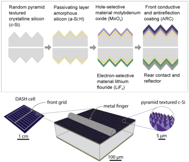 In this illustration, the top images show a cross-section of a solar cell design that uses a combination of moly oxide and lithium fluoride. These materials allow the device to achieve high efficiency in converting sunlight to energy without the need for a process known as doping. The bottom images show the dimensions of the DASH solar cell components. (Image credit: Nature Energy 10.1038/nenergy.2015.31)
This new mix of materials - which could also be used in semiconductor components - prevents the necessity for a doping process, which introduces foreign atoms to the electrical contacts of the device. The doping process deteriorates the performance of the device and also adds complexity.
The solar cell industry is driven by the need to reduce costs and increase performance. If you look at the architecture of the solar cell we made, it is very simple. That simplicity can translate to reduced cost. Conventional silicon solar cells use a process called impurity doping, which does bring about a number of limitations that are making further progress increasingly difficult.
James Bullock, Lead Author, Australian National University
Bullock participated in the study as a visiting researcher at the U.S. Department of Energy’s Lawrence Berkeley National Laboratory (Berkeley Lab) and UC Berkeley.The other scientists who participated in the study were from The Swiss Federal Institute of Technology of Lausanne (EPFL), ANU, UC Berkeley, and Berkeley Lab.
Currently, silicon wafers are used in a number of solar cells. Atoms are doped on the wafer, and sometimes even on the layers placed on the wafer. The atoms either have spare electrons when they bond with silicon atoms, or they generate electron deficiencies or "holes." Electrical conductivity is improved by this doping process.
These devices require two different types of dopant atoms at the electrical contacts of the solar cell. This is to control how the holes and the electrons move in a solar cell so that the conversion of sunlight into electricity is successful.
Crystalline silicon-based solar cells featuring doped contacts exhibit conversion efficiency of more than 20%. Previously, a dopant-free silicon cell did not exceed 14% conversion efficiency.
The researchers have been successful in demonstrating the dopant-free silicon cell - also known as dopant free asymmetric heterocontact (DASH) cell - which is more than 19% efficient on an average level. This increased efficiency is the outcome of the new materials and a coating process that is used for layers on the bottom and top of the device. These researchers have illustrated that it is possible to develop solar cells in just seven steps.
As part of the study, the team used a crystalline silicon core with dopant-free type silicon layers known as amorphous silicon. Ultrathin coatings of molybdenum oxide, also called moly oxide, were then applied at the bottom surface of the lithium fluoride and also at the solar cell’s side that faces the sun. The two layers, with a thickness of tens of nanometers, are used as dopant-free contacts for electrons and holes.
Moly oxide and lithium fluoride have properties that make them ideal for dopant-free electrical contacts.
Ali Javey, Program Leader, Electronic Materials, Berkeley Lab
Lithium fluoride and moly oxide are transparent, and they have very supportive electronic structures appropriate for solar cells.
They were previously explored for other types of devices, but they were not carefully explored by the crystalline silicon solar cell community.
Ali Javey, Program Leader, Electronic Materials at Berkeley Lab
Javey highlighted that the research team had already discovered the advantage of using moly oxide as a hole contact suitable for crystalline silicon. “It has a lot of defects, and these defects are critical and important for the arising properties. These are good defects,” he said.
We have adapted the technology in our solar cell manufacturing platform at EPFL and found out that these moly oxide layers work extremely well when optimized and used in combination with thin amorphous layer of silicon on crystalline wafers. They allow amazing variations of our standard approach.
Stefaan de Wolf, Team Leader, Crystalline Silicon Research, EPFL
The team finally discovered lithium fluoride to be an efficient candidate for electron contacts to crystalline silicon containing a thin amorphous layer coating. The layer of moly oxide for hole contacts is complemented by this thin amorphous layer.
Moly oxide and lithium fluoride layers were deposited for the new solar cell through thermal evaporation, which is a room-temperature method. The team hopes to test many other materials to monitor whether they can help enhance the efficiency of the solar cell.
There’s a critical need to reduce the contact resistance in transistors so we’re trying to see if this can help.
Ali Javey, Program Leader, Electronic Materials at Berkeley Lab
Some off the work in this study was performed at The Molecular Foundry, a DOE Office of Science User Facility at Berkeley Lab.
This work was supported by the Bay Area Photovoltaics Consortium (BAPVC); DOE Office of Science; a DOE Energy Innovation Hub; the Australian Renewable Energy Agency (ARENA); Office fédéral de l’énergie (OFEN); the CSEM PV-center; and the Joint Center for Artificial Photosynthesis.