Perovskite materials have received a lot of attention due to their exceptional optoelectronic characteristics. Perovskite solar cell technology is also considered very promising when used in flexible solar cells and tandem solar cells.
Lead halide perovskite materials were first used in solar cells in 2009, achieving a photoelectric conversion efficiency (PCE) of 3.8%.1 In recent years, after optimizing the component control, interface control, defect passivation, energy level control, and transport layer of the solar cell device, the PCE was increased to 26.7%.2
The tandem solar cell, which combines perovskite and Si-based solar cell technologies, has the potential to achieve a PCE of 33.9%.2
According to research on perovskite solar cells, the quality of the device's key layers influences the cell's PCE. Hence, monitoring the thickness and uniformity of these layers is critical.
Accurate and fast thickness measurement of these layers can be difficult. White light interferometer measurements have an optical offset and are related to different materials. The reflectometer cannot measure non-transparent metal layer thickness and requires complex modeling for other ultra-thin transparent film measurements. The AFM has a restricted scan range and low throughput.
The KLA Instruments™ Tencor® P-Series stylus profilers use a linear variable differential capacitor (LVDC) sensor, which minimizes friction and self-heating effects.
Along with high vertical resolution and measurement repeatability, KLA Instruments stylus profilers provide exceptional performance and dependability for layer thickness measurements ranging from sub-10nm to hundreds of nm.
As a result, the stylus profiler provides an effective method for perovskite manufacturers to monitor their operations, which is the focus of this article.
Perovskite Solar Cell Device Structure
A Perovskite Solar Cell (PSC) Device has a simple structure with several layers for various functions: the substrate, the electron transport layer (ETL), the perovskite material layer, the hole transport layer (HTL), and the metal electrode layer.
PSCs are typically classified into two types: n-i-p and p-i-n. The ETL and HTL are positioned in separate positions on the device structure. The "n" symbolizes the ETL, the "i" stands for the perovskite layer where light is absorbed and an electron-hole pair is formed, and the "p" stands for the HTL.
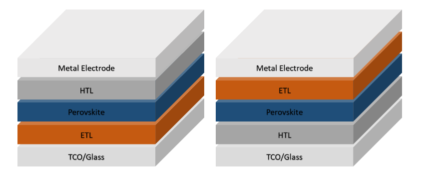
Figure 1. “n-i-p” (left) and “p-i-n” (right) structure of a perovskite solar cell device. Image Credit: KLA Instruments™
Figure 1 shows the structure of typical “n-i-p” (left) and “p-i-n” (right) perovskite solar cell devices. When different materials are applied to these layers, the “n-i-p” or “p-i-n” structure affects the device's performance and lifetime.
Principle of the Perovskite Solar Cell Device
Figure 2 shows how a PSC device operates, with the p-i-n structure as an example. First, the perovskite layer absorbs photons with energy greater than the band gap of the perovskite material and produces excitons (electron-hole pairs) via the coulomb force.
Since the excitons are in an electric field, they migrate to the interface between the perovskite and transport layers. Because the exciton binding energy of the perovskite material is low, the exciton is rapidly dissociated into a hole and an electron.
The divided electrons and holes would eventually travel to the cathode and anode via the electron transport layer (ETL) and hole transport layer (HTL). This process creates photovoltage and photocurrent, and the photoelectric conversion process is carried out via an external circuit.
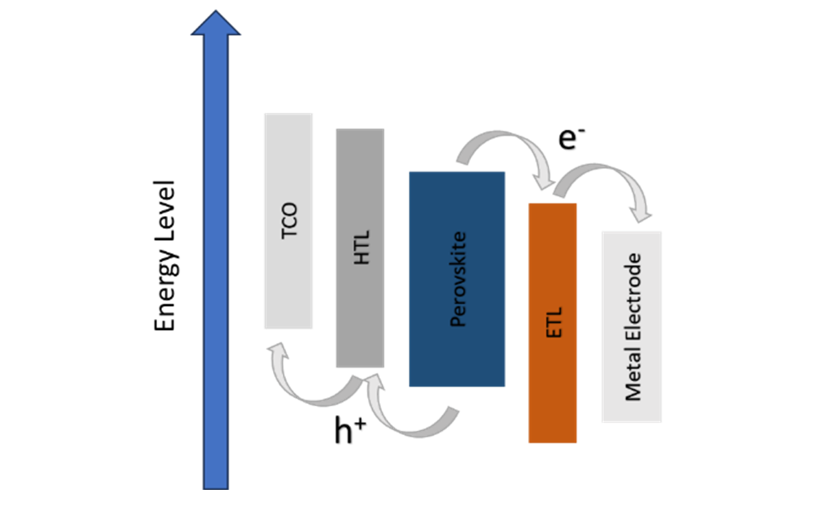
Figure 2. PSC device working principle schematic. Image Credit: KLA Instruments™
Perovskite Solar Panel Manufacturing
The basic structure of a perovskite solar panel is identical to that of a single solar cell, but extra etching is required to divide the large panel into smaller cells and connect them together. Figure 3 shows the simplified manufacturing process for the perovskite solar panel.
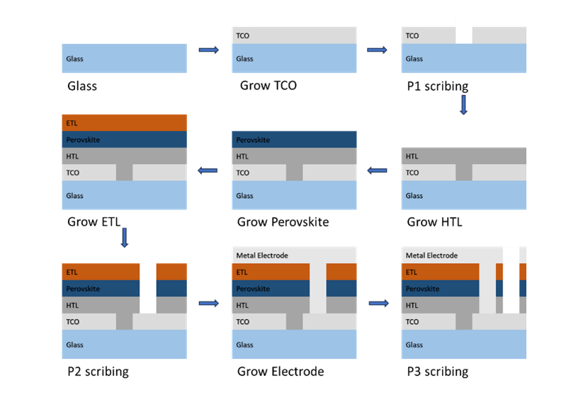
Figure 3. Simplified manufacturing process of the perovskite solar panel. Image Credit: KLA Instruments™
P1 scribing separates the TCO anode into tiny cells, whereas P2 scribing eliminates the ETL, perovskite, and HTL materials, revealing the TCO anode. Next, the single cells are connected in series by inserting the top metal electrode into the P2 line. Finally, P3 scribing separates the upper cathode into individual cells.
Ultra-Thin Film Measurement with KLA P-Series Tools
The primary goal for all solar cell producers is to reduce material costs while increasing photoelectric conversion efficiency. The most straightforward approach for perovskite-based technology is to lower film thickness, particularly for TCO, ETL, and HTL.
The Tencor P-series profilers work well when measuring samples with nm-scale thicknesses. The three studies below look at distinct layers with varying thicknesses.
Study 1: 3D Topography and Step Height of TCO Layer
The TCO layer is a PSC device's first and most critical layer. To increase the device's PCE, the TCO material must be high in light transmittance, low in resistivity, and thermally stable.
Fluorine-doped tin oxide (FTO), indium-doped tin oxide (ITO), indium-doped zinc oxide (IZO), and aluminum-doped zinc oxide (AZO) are commonly used as TCO layer materials.
Figure 4a depicts a three-dimensional measurement of the 6.8 nm thick IZO layer on a glass substrate. Figure 4b shows the 2D measurement results for the same sample, whereas Figure 4c compares two IZO samples with thicknesses of 6.8nm and 37.1nm.
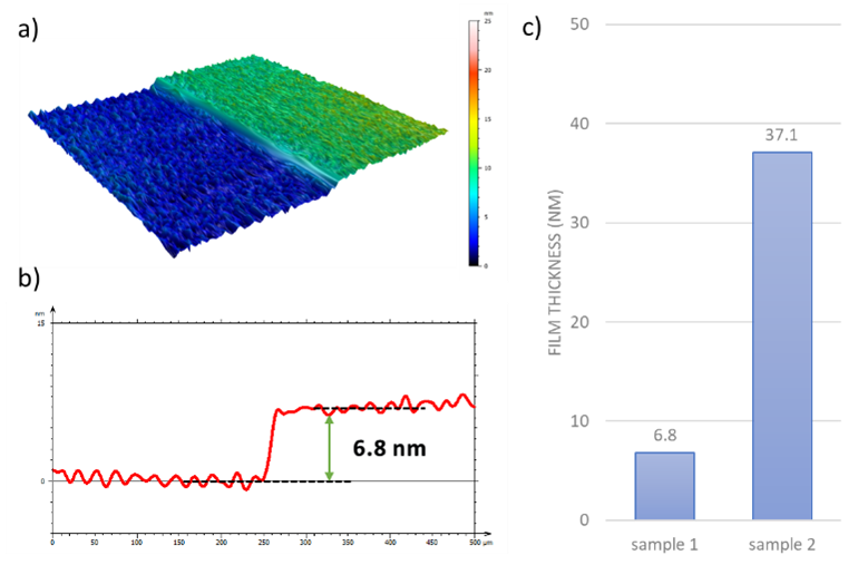
Figure 4. (a) the 3D image of the 6.8 nm IZO layer on a glass substrate; (b) the 2D scan result from the same sample; and (c) two IZO samples measured with thicknesses of 6.8nm and 37.1nm. Image Credit: KLA Instruments™
Study 2: 3D Topography and Step Height of the ETL Layer
The ETL layer is important in the PSC device. The main functions of ETL are:
- Gathering electrons and transporting them to the electrode.
- Transporting electrons but blocking holes to decrease the electron-hole recombination rate.
- In the "n-i-p" structure, the perovskite layer is grown on ETL, thus the flatness and surface roughness of the ETL layer directly impacts the quality of the perovskite layer.
- In the "p-i-n" structure, the ETL layer is also a protection layer of the perovskite from erosion of water and oxygen.
As a result, it is critical to check the thickness and consistency of the ETL layer.
SnO2 is the most commonly utilized ETL material in PSC devices, followed by titanium dioxide (TiO2), niobium pentoxide (Nb2O5), zinc oxide (ZnO), and cadmium sulphide (CdS).
Figure 5a depicts the three-dimensional image of a 10.2 nm thick SnO2 layer on a glass substrate. Figure 5b shows the 2D measurement results for the same sample, whereas Figure 5c compares three SnO2 samples with thickness measurements of 10.2 nm, 14.3 nm, and 19.6 nm.
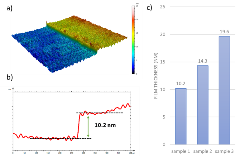
Figure 5. (a) the 3D image of 10.2 nm SnO2 layer on a glass substrate; (b) the 2D scan result from the same sample; and (c) three SnO2 samples measured with thicknesses of 10.2 nm, 14.3 nm and 19.6 nm. Image Credit: KLA Instruments™
Study 3: 3D Topography and Step Height of Metal Electrode Layer
The metal electrode layer forms the top layer of the PSC device. It must have a stable and homogeneous coating substance because it is immediately exposed to the outside environment. Metal electrodes often consist of Au, Al, or Ag. Creating a thin and uniform metal electrode layer is an important step in lowering device costs.
Figure 6a depicts a 3D picture of a 15.0 nm thick Al layer on a glass substrate. Figure 6b depicts the 2D scan results from the same material, whereas Figure 6c compares four measured metal films ranging in thickness from 15.0 nm to 71.1 nm.
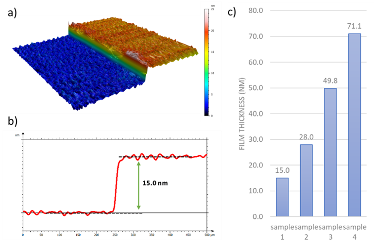
Figure 6. (a) the 3D image of a 15.0 nm thick Al layer on a glass substrate; (b) the 2D scan result from the same sample; and (c) four metal samples measured with thicknesses of 15.0 nm to 71.1 nm. Image Credit: KLA Instruments™
Conclusions
Perovskite and tandem solar cell device technologies are increasingly used in the solar sector. The KLA Instruments™ Tencor® P-series stylus profilers offer perovskite device manufacturers a powerful option for measuring ultra-thin film thickness and monitoring homogeneity. They have great vertical resolution and outstanding measurement repeatability, even for nanometer-scale steps.
Reference
- Kojima, A., et al. (2009). Organometal Halide Perovskites as Visible-Light Sensitizers for Photovoltaic Cells. Journal of the American Chemical Society, 131(17), pp.6050–6051. https://doi.org/10.1021/ja809598r.
- Cell Efficiency (%) 12 8 4.

This information has been sourced, reviewed and adapted from materials provided by KLA Instruments™.
For more information on this source, please visit KLA Instruments™.