As nations worldwide aim to lower carbon emissions and adopt sustainable energy resources, the solar energy industry has undergone substantial growth. Among the various crystalline silicon (c-Si) process routes, Tunnel Oxide Passivated Contact Solar Cells (TOPCon) stand out for their high photovoltaic conversion efficiency (PCE) and cost-effectiveness.1
The highest PCE reached by an industrial TOPCon cell is 25.42 %, approaching the theoretical limit of approximately 29 %.1,2 Pursuing higher PCE values is the latest challenge in both process control and tracking.
As with other c-Si solar cell processes, doping level monitoring is essential for managing TOPCon process quality, as solar cell performance relies on a delicate balance between conductivity, contact resistance, and recombination rate, all of which are significantly influenced by the doping level of the material.
Multiple test methods, including carrier lifetime measurement and photoluminescence imaging, transform microwave or optical signals into carrier density data. However, these indirect testing techniques require complicated calibration and are easily influenced by external interference.
In contrast, four-point probe (4PP) sheet resistance (Rs) measurements provide direct electrical characteristics like carrier mobility and contact resistance, making it a vital method for TOPCon process monitoring.
Since the release of the first four-point probe (4PP) system in 1984, KLA has been a pioneer in resistivity measurement innovation. Its Rs measurement systems are widely recognized in the semiconductor industry.
The KLA Instruments™ Filmetrics® R54 sheet resistance mapping system is a benchtop Rs platform featuring the latest KLA Rs test probes and measuring circuits. This study presents the 4PP measurement method and details the current TOPCon solar cell process. Rs data from multiple TOPCon processes shows that the R54 provides an exceptional solution for TOPCon process monitoring.
Four-Point Probe Measurement in Solar Cells
The 4PP method has remained popular for over 100 years because of its accuracy and simplicity. In a four-point probe measurement, electrical current is passed between two pins in contact with a conductive surface, and the voltage is measured between two additional pins also in contact with the surface, as illustrated in Figure 1.
The standard measurement setup on the left is used for applications where the test area is positioned away from the sample edge. For measurements performed close to the sample edge, an additional measurement may be taken using the alternate setup on the right as part of the Dual Configuration approach. This approach eliminates the edge effect by adding a calibration coefficient based on the resistance RA and RB obtained from both data points.
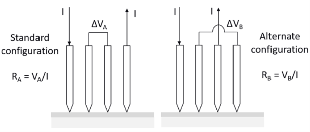
Figure 1. Four-point probe pin schematic for both the standard (left) and alternate (right) linear configurations. Image Credit: KLA Instruments™
In addition to the common 4PP configuration, the R54 features multiple essential features that provide substantial benefits for solar cell testing, including:
- An opaque measuring chamber (Figure 2, left) is used to eliminate photocurrent generation.
- A square chuck (Figure 2, right) specially designed for holding square-shaped solar samples.
- Compatibility with all KLA sheet resistance probes.
- Auto current adjustment according to a target voltage.
- Dynamic correction for edge effects and tip geometry.
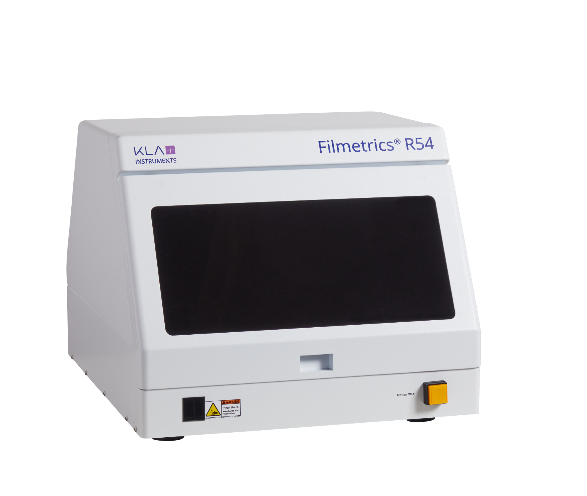
Figure 2. The R54 sheet resistance mapping system (top), and a solar cell mounted on the square chuck designed for solar cell applications (bottom). Image Credit: KLA Instruments™
TOPCon Solar Cell Architecture and Process
Crafted from n-doped silicon, TOPCon solar cells feature multiple-layer structures on both front and rear sides, as demonstrated in Figure 3.
On the front side, the p-type emitter is formed on the textured Si surface to facilitate photo-generating carrier collection. The emitter layer is covered by a composite passivation layer that reduces the recombination rate, while the front surface is topped with a SiNx anti-reflective (AR) layer and metal electrodes.
On the rear side, the TOPCon solar cell incorporates a SiOx/n-poly silicon passivation layer, which allows one carrier type to tunnel while blocking the other. This passivation layer lowers the interface recombination rate and increases the open circuit voltage, boosting efficiency.
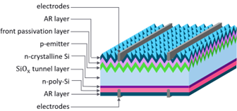
Figure 3. Structure of a TOPCon solar cell. Image Credit: KLA Instruments™
Figure 4 depicts an up-to-date TOPCon process flow. Crystalline n-doped silicon wafers are first alkali-textured to create pyramid structures on the front surface, after which a boron emitter is produced to form a p-n junction with the n-doped substrate.
Following this, an oxidation process drives in the boron atoms and adjusts the junction depth. The wafer’s rear surface is then etched by hydrofluoric acid and alkali to achieve a flat Si interface.
Following residue removal, a thin oxide (SiOx) tunnel layer is thermally grown on the rear surface, after which a phosphorus-diffused polycrystalline silicon serves as the passivation layer. Fabrication of the rear surface passivated contact is completed through an annealing process. Heating the wafer during this process redistributes impurities into a stable state while fixing harmful ions such as sodium and potassium.
The remaining stages in the TOPCon process resemble those in passivated emitter and rear contact (PERC) or other c-Si based solar cell processes: buffered oxide etch (BOE) cleaning eliminates oxidation layers, exposing a fresh silicon surface on both sides of the wafer. This is followed by sequential coating of the front passivation and AR layers.
Front surface metallization concludes the process flow. Laser pulses assist the sintering of silver contacts, creating a highly doped region to obtain reduced contact resistance. This procedure is referred to as laser-enhanced contact optimization (LECO).
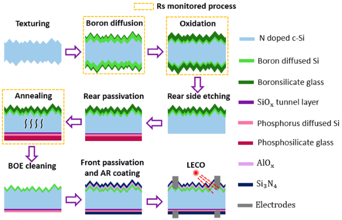
Figure 4. Process flow of TOPCon solar cell. Image Credit: KLA Instruments™
Rs Monitoring Using the Filmetrics R54
Boron diffusion, oxidation, and annealing in a TOPCon manufacturing line involve either direct doping processes or thermal treatment that can alter sample doping levels, making accurate Rs monitoring crucial. The KLA Instruments Filmetrics R54 sheet resistance mapping system has demonstrated full capability for Rs monitoring in these three processes.
Rs Mapping of TOPCon Solar Cells
Rs mapping provides a direct method for delivering spatially resolved information on dopant diffusion uniformity. Mapping Rs across the entire wafer can identify inconsistencies in doping level, defects, or unexpected wrap coating.
The R54 offers customizable test patterns within a maximum measurement size of 200 mm x 200 mm. Figure 5 presents three 225-point Rs maps of a TOPCon cell following the boron diffusion, oxidation, and annealing processes.
The testing probe penetrates the surface oxidation layer for precise Rs measurement. Rs distribution data from boron diffusion and oxidation is more variable than data from annealing due to the greater complexity of boron doping compared to phosphorus.
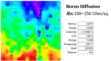
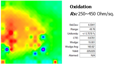
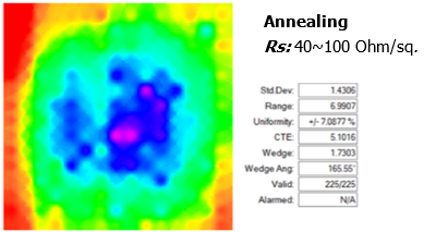
Figure 5. 225-point sheet resistance maps of boron diffusion (top), oxidation (center) and annealing (bottom) processes. Image Credit: KLA Instruments™
The R54 software interface displays statistical results upon completion of Rs mapping. The two most important values in process control are the mean Rs value and uniformity. Uniformity is defined as (max Rs – min Rs)/(2*mean Rs), the standard definition adopted by the solar industry.
Reliability of Rs Measurements
The majority of TOPCon manufacturing lines include integrated in-line Rs monitoring instruments, which require an extremely precise and stable off-line Rs golden instrument to ensure accurate calibration and alignment of all in-line Rs monitors. The Filmetrics R54 is one of the most competitive Rs golden instruments in the solar industry, with Rs test reliability verified through repeatability and long-term stability testing.
An in-depth analysis was performed using 10 wafers for each process to evaluate the repeatability of Rs measurements. Each wafer was mapped 10 times to determine its average Rs, with repeatability indicated by the standard deviation of these averages (refer to the zoom-in view of Figure 6a).
As illustrated in Figure 6, the repeatability values for boron diffusion wafers (Figure 6a) are under 0.5 % of the average Rs. For oxidation (Figure 6b) and annealing wafers (Figure 6c), repeatability values are all under 0.3 % of the average Rs. These results are significantly below the process monitor thresholds.
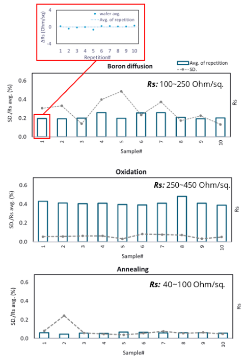
Figure 6. Repeatability of measured sheet resistance on ten wafers for boron diffusion (top), oxidation (center), and annealing (bottom). The inset in the top graph shows the Rs variation for a 10x measurement. Image Credit: KLA Instruments™
Rs monitoring was conducted across the three processes over four weeks to demonstrate long-term stability. The Rs values were tested once every two weeks, with results shown in Figure 7. For the five samples chosen from each process, Rs variation across four weeks measured < 1 % of the wafer average, signifying stable long-term performance within the anticipated range of the samples’ natural Rs fluctuations. Data on repeatability and long-term variation is outlined in Table 1.
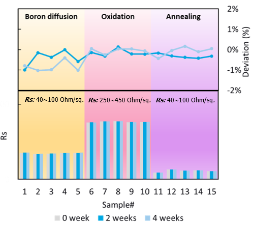
Figure 7. Long-term stability of Rs on five samples of each of the three processes, measured over a four-week period. Image Credit: KLA Instruments™
Table 1. Repeatability and long-term variation in different processes. Source: KLA Instruments™
| Process |
Repeatability |
Long-term variation |
| Boron diffusion |
0.3 % |
1.0 % |
| Oxidation |
0.1 % |
0.2 % |
| Annealing |
0.1 % |
0.1 % |
Conclusion
As TOPCon technology continues to push the boundaries of c-Si photovoltaic efficiency, accurate sheet resistance monitoring remains essential for high-quality process control. The KLA Instruments™ Filmetrics® R54 system delivers detailed sheet resistance mapping with excellent repeatability and long-term stability.
Equipped with a solar cell chuck, the R54 offers full capability for TOPCon solar cell sheet resistance measurement, with performance verified for actual manufacturing processes.
References and Further Reading:
- Feldmann, F., et al. (2014). Passivated rear contacts for high-efficiency n-type Si solar cells providing high interface passivation quality and excellent transport characteristics. Solar Energy Materials and Solar Cells, 120, pp.270–274. https://doi.org/10.1016/j.solmat.2013.09.017.
- Richter, A., Hermle, M., and Glunz, S.W. (2013). Reassessment of the Limiting Efficiency for Crystalline Silicon Solar Cells. IEEE Journal of Photovoltaics, 3(4), pp.1184–1191. https://doi.org/10.1109/jphotov.2013.2270351.
This information has been sourced, reviewed, and adapted from materials provided by KLA Instruments™ .
For more information on this source, please visit KLA Instruments™.