Mar 16 2009
Applied Materials, Inc. today released its Applied HCT MaxEdge™ wire saw, a new platform for slicing ingots into ultra-thin wafers that can help customers drive down the cost of manufacturing photovoltaic (PV) cells by up to $0.18 per watt.* Key technical advances, including an industry-first dual-wire management system, enable the MaxEdge system to deliver significantly higher throughput and load capacity than competitive systems, while requiring much less factory floor space and fewer operators for equivalent megawatt output.
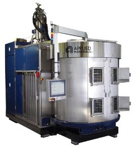 The new Applied HCT MaxEdge wire saw can help customers reduce the cost of manufacturing photovoltaic cells by enabling larger loads and using thinner wires at higher cutting speeds
By making thinner wafers, PV cell manufacturers can reduce the amount of silicon per wafer and lower the cost-per-watt of solar electricity. To produce thinner wafers, traditional wire saws must reduce the ingot length (load) and the cutting speed. The uniquely designed MaxEdge system delivers ultra-thin wafers without sacrificing throughput by enabling larger loads and using thinner wires at higher cutting speeds.
“With the MaxEdge system we’ve boosted the wafer output and lowered the operating expenses of our industry-leading Applied HCT B5 system, making the best wire saw on the market even better,” said Stefan Schneeberger, vice president and general manager of Applied Materials’ Precision Wafering Systems division. “The MaxEdge system builds on a 25-year history of wire saw innovation and incorporates key feedback from our customers. Since the wafer is the most expensive component of crystalline silicon-based PV manufacturing flow, reducing wafer fabrication cost is critical to the goal of making solar energy competitive with grid power.”
The MaxEdge system’s breakthrough dual-wire management system employs four independently-controlled direct drive motors and advanced process control to lower wire tension, reducing wire wear and decreasing ingot scrap and unplanned downtime. Reduced tension also allows smaller diameter cutting wires to be used, resulting in significantly less silicon loss without compromising yield. For more information, please visit http://www.appliedmaterials.com/products/maxedge_3.html
The MaxEdge system is part of Applied’s portfolio of production-proven systems for ultra-thin crystalline silicon solar cells, including the Applied ATON™ PVD system for anti-reflective and passivation layer deposition and the Applied Baccini Soft Line™ integrated system for all-in-one screen printing, edge isolation, test and sort.
Applied Materials, Inc. (Nasdaq:AMAT) is the global leader in Nanomanufacturing Technology™ solutions with a broad portfolio of innovative equipment, service and software products for the fabrication of semiconductor chips, flat panel displays, solar photovoltaic cells, flexible electronics and energy efficient glass. At Applied Materials, we apply Nanomanufacturing Technology to improve the way people live.