Feb 14 2011
Engineers working at the Berkeley, University of California, have developed a process whereby nanolasers could be grown directly on a silicon surface. This technique could in the long run lead to on-chip fabrication of nanophotonic instruments such as solar cells.
The nanolasers are the resultant of a mission to capture the ability of light to carry data in a better manner. These could later be used for smaller and faster computer chips. Most silicon based electronics are poor at light generation. Hence engineers have long been trying to use III-V for creating light- based components. However, blending III-V with silicon for creation of a single optoelectronic chip has been very difficult .They found it extremely difficult to overcome the mismatch of the two materials¡¦ atomic structures and fabricating electronics on a large scale basis without the proper infrastructure, which meant undertaking huge investments.
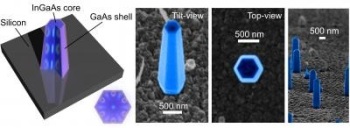 Nanopillar
According to Connie Chang-Hasnain, Professor of computer sciences and electrical engineering at UC Berkeley, it was extremely hard to change the present day huge silicon electronics infrastructure both technologically and economically. Hence it was critical that they should be compatible with silicon fabrication. Normally temperatures ranging above 700° Celsius are required for the growth of III-V semiconductors. Such high temperatures are needed to eliminate the electronics and other integration processes. The scientists at the UC Berkeley have surmounted this difficulty by identifying a method of growing nanopillars made from indium gallium arsenide, which is a III-V material on a silicon surface at a comparatively cool temperature of 400° Celsius. The method uses metal organic chemical vapor deposits to grow the nanopillars on the silicon. This method is already in use for commercial production of thin film solar cells and LEDs.
The nanopillar lasers that were thus developed had the capacity to generate 950 nm light at ordinary room temperatures. According to the researchers, this method could also facilitate development of super efficient silicon photonics. The miniature size of nanopillars, smaller than one wavelength on each side, makes it easy for packing into small spaces and they have an added advantage of using very little energy. Roger Chen, a graduate electrical engineering student in the UC Berkeley, mentioned that this technique would probably be a new opportunity for engineering on-chip nanophotonic instruments such as photodetectors, lasers, solar cells and modulators.